~ 公怖欄 ~

本部落格文章已停止更新,大部分的文章皆已轉移轉移至
電子製造,工作狂人(ResearchMFG)新站。
此網站將不再回答任何訪客留言~

顯示具有 FPC 標籤的文章。 顯示所有文章

2008年10月11日 星期六

[技術] 簡介PTF(Polymer Tick Film)聚合厚模

PTF: Polymer Thick Film (聚合厚膜)

PET: Polyethylene terephthalate (聚乙烯對苯二甲酸酯),維基的解釋

聚合厚膜(PTF)軟性電路板:
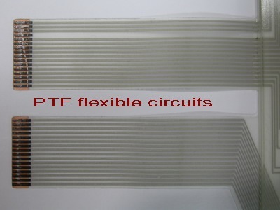
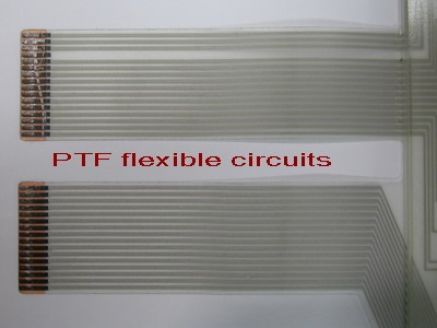
利用網板印刷(silkscreen)把一層導電油墨(conductive_layer)及一層絕緣油墨(dielectric layer)印刷於PET基材上所形成的。通常是單層的線路,也可以是雙層或是多層線路,中間透過印刷或是經由類似通孔的印刷連結導電層與導電層。

(↓PTF的成型品)
PTF_sample_thumb1

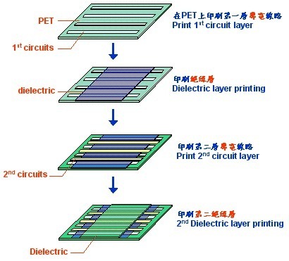
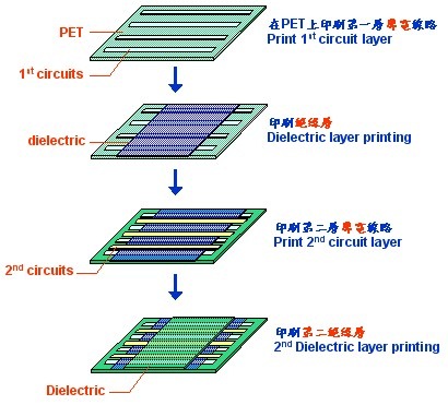
雙層油墨的製造流程:

步驟一,印刷層導電線路於PET的基材上,有些PET會作霧化處裡以增加其導電油墨的附著力。點電油墨通裡使用銀漿導電石墨當作主要成分,所以會比一般的軟性電路板的鍍金要來得便宜。

步驟二,印刷層絕緣油墨並覆蓋在第一層導電線路上,以避免與第二層導電線路短路,但須預留下要與第二層導電線路連通的線路,不可覆蓋。絕緣層通常使用UV油墨為材質,因為可以快速烘乾,所以印刷完要經過UV燈烘烤。

步驟三,印刷層導電線路於層絕緣油墨上,留意與層導電線接觸的地方。

步驟四,印刷層絕緣油墨並覆蓋所有的導電線路,如有導電及特殊需求例外。

FTP_process02_thumb1

PTF的優點

  • 價錢較低並符合環保: PTF軟性電路板由於使用銀漿導電石墨並利用網板印刷來完成線路的佈局,比起一般傳統的軟性電路板使用銅板及電鍍金製程來得便宜很多。而且沒有電鍍製需求更為環保。
  • 交期短: 既然沒有電鍍製程,其製作流程比起傳統的軟性電路板少了很多的步驟及乾燥的時間。

PTF的缺點

  • 不可對折: FPC由於是使用銀膠及石墨的印刷,延展性比不上銅、金,強烈建議不可對折PTF軟性電路板。
  • 線路的間隙有最小限制: PTF廠商宣稱最小的線路間的間隙(space)為5mils (0.127mm),但是不良率非常高;一般的建議最小線路間的間隙(space)為20mils (0.5mm) 。傳統軟性電路板的最小的線路間的間隙(space)為3mils。

延伸閱讀:
PTF(Polymer Thick Film)製造的製程能力
PTF在PET上印刷線路的注意事項
軟性電路板(FPCB)線路設計注意事項 I

2008年9月16日 星期二

[技術] PTF(Polymer Thick Film)製造的製程能力

PTF由於使用絲印(screen Printing)製程來印刷導電線路,所以其製程的精準度無法和FPC的蝕刻製程相比擬。

下面是我所知道的PTF的製程能力,僅供參考

層於層之間的印刷對位經準度:0.05mm (最小)

定位孔的精準度:0.02mm(最小)

外型裁切的偏移精準度:0.05mm (最小)

所以,整體的導電線路最小印刷偏移量為 0.12mm = 0.05+0.02+0.05 (適用於兩層導電層以上的的產品,如果是單層線路,最小偏移量為0.07mm)


延伸閱讀:
PTF在PET上印刷線路的注意事項

2008年9月15日 星期一

[技術] FPC 結構 (資料收集)

在網路衝浪時,發現一些與FPC相關且有用的網站,在這裡先記錄下其網址以便日後所需。

Single Sided Flexible Circuit:

Solder Resist Type of Single Sided FPC

Double Access Flexible Circuit:

dual access fpcDual Access Flex Circuit

Double Sided Flexible Circuit:

Double Sided FPC StructureDouble Sided FPCs Samples

Multi-layer Flexible Circuit:

Multi Layer FPC Structure

FPC ability

Parameter (mm)
Polyimide (PI)
PET
Laminate Thickness 0.025 / 0.050/ 0.125/ 0.175 0.025 / 0.050/ 0.075
Copper Foil 0.018,0.035,0.070 0.035,0.070
Min Pattern width/Space 0.075(3 mil) 0.075(3 mil)
Min. Drilled Hole Size Non-Plated Thru 0.25 ( .010" ); Tolerance +/-.0386( .0015")
Plated Thru

0.25. ( .010" ); Tolerance +/-.076( .0030")

Outlines Dimension +/- 0.05 +/- 0.05

Peeling Strength(180°Direction)

>1.2kgf / cm >1.2kgf / cm
Solder Hent Resistance 280℃ / 10secs 280℃ / 10secs
Surface Treatment Ni/Au 2~5μm 2~5μm
Au(Electro/Immersion) 0.03 ~0.1μm 0.03 ~0.1μm
Sn/Pb (Lead Free) 3~ 20μm 3~ 20μm
Sn-Cu Plating (Lead Free) 3~ 5μm 3~ 5μm
Tin Plating (Pure Sn) 5 ~ 8μm 5 ~ 8μm
Bending flexibility Meet to IPC Criterion
Chemical Resistance Meet to IPC Criterion

這裡有一個關於[軟性線路板 - FPC]的網站,有提到很多的FPC的觀念,只可惜是簡體字,改天慢慢咀嚼後在撰文與大家分享。http://www.bestfpc.com/fpcblog/cn/

2008年9月12日 星期五

[技術] PTF在PET上印刷線路的注意事項

PTF: Polymer Thick Film (聚合厚模),

PET: Polyethylene terephthalate (聚乙烯對苯二甲酸酯),維基的解釋

就如同大家所知道的,相較於FPC,PTF軟板的確有其低價、交期短的諸多優點,但是PTF卻有其先天上的能力限制。由於使用絲網印刷製程的緣故,PFT無法製作比FPC還小的電子線路間距,雖然宣稱可以達到最小5mils (0.12mm)的電子線路間距,但其實10mils(0.25mm)就已經快到極限。另外,PTF也無法承受對折式的壓折,因為其電子線路的材質為銀漿及導電碳,它門沒有如FPC的銅線路具有延展的能力,可以承受少次數的彎折。

下面會就個人使用PTF的經驗,提出PTF在製作上的製程能力限制及解決方法。

  • 異物沾污:不導電的異物(particle),如果沾黏於電子線路之上,其最小的影響是增加線路的電阻值,因為電阻值與電子通過的面積成反比,並很有可能造成電性開路(open);如果是具導電性的異物沾污於線路及線路之間,就很有可能會造成電性短路(short),這種缺點最讓人討厭了,因為它在製造工廠生產時,沒有辦法完全透過測試的方法篩選出來,通常必須等到安裝於產品一段時間後才會產生問題,尤其是使用於高溫又高濕的地區。以後如果有機會,可以再撰文談討這個主題。
    異物可能來自環境中的空氣,有灰塵、纖維、紙屑等。一般來說都是人為的異物,如衣服上就有很多的纖維,特別是毛衣或是棉質的衣服。瓦愣紙箱也是一大污然來源,有毛屑、紙屑及纖維。最好的防治知道是,設置一個100K等級的
    潔靜室(Clean room),人員穿著防塵衣,並嚴格控制各種可能的污染源。環境控制的重要性,特別是在生產小間距線路的產品時。
    另外一個異物的可能來源是油墨,油墨在製作會加入一些金屬成份的添加劑,這些添加劑如果管控不當,很有可會結成硬塊,較大的硬塊無法流經絲網印的網目,就會阻塞絲印的網目,而造成印刷缺孔,甚至是造成電子線路斷線;較小的硬塊可以流經網目,但會在電子線路上形成凸點,這時如果有重疊的上、下層線路時,凸點很有可能會穿破絕緣層(dielectric layer)而造成上、下線路短路。油墨的污染也可能來自於油墨生產時的不良環境空氣,或是油墨存放的環境。管控油墨異物最好的方法是,用適當大小的濾網過濾油墨的沾污;如果沾污嚴重時,也可以先用粗濾網後用細濾網。
  • 導電層的印刷沾污:絲網印刷時,導電油墨的黏稠度相當重要,當稀釋劑添加太多時,油墨就會變稀 而變得容易滲透到原本不應該印有油墨的地方,這種缺點稱為印刷沾污,更糟糕的是這種沾污會持續到下一次印刷,甚至是下下一次,直到沾污的油墨乾竭為止。嚴重的印刷沾污會直接造成相鄰導電線路間的短路;輕微的印刷沾污也可能會影響到線路與線路間的電子流動,如果加上電壓為能源、溼度為催化劑,就很可能產生電子遷移(eletromigration)現象於線路與線路之間,隨著時間一久,就會產生導電性造成短路。
    解決這種導電層印刷沾污的方法,其一是選用適當油墨並控制稀釋劑的添加;其二是定期清洗絲印網板;其三是加強檢查,最好是每做好一張就檢查一張,如果能有AOI(Auto Optical Inspector,自動影像檢測機)就更好了。
     
    PTF_Print_smear_s
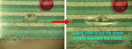
    (↑上圖為導電線路印刷沾污,經一段時經使用後沾污擴散,並造成電子短路,用刀片把沾污的地方割開後,電器特性就恢復正常。)
  • 絕緣層的印刷孔、洞:絲印網板是由經線及緯線所構成,既然是線所構成,在印刷時有線的地方就會有印刷不到的地方,尤其是在經線及緯線交叉的地方,就會形成印刷不到的孔洞,這些孔洞極為細微,很難用眼睛觀察到,但電子還是有可能穿過,這時如果孔洞剛好落在相鄰層的導電線路上,就會造成層與層之間的短路。 
    silkscreen_mesh02
    解決這種絕緣層印刷孔、洞的方法,可以降低絕緣層油墨的黏度,讓絕緣油墨可以滲透到經、緯線底下(※請注意:不要把導電油墨的增加黏度與絕緣層降低黏度搞混了)。另外的方法,是增加絕緣層印刷的次數的2~3層,並規定每一絕緣層都使用不同網目及經緯方向的絲印網板,目的是讓不同的網板印刷可以互相填補孔洞。

延伸閱讀:
Hot-Bar 軟板設計注意事項
FPC Trace Pattern Layout Design Notices (軟板線路設計注意事項)
PTF(Polymer Thick Film)製造的製程能力
簡介PTF(Polymer Tick Film)聚合厚模

[Tech.] Notices for Screen-Printing on PET

The PTF (Polymer Thick Film) uses silkscreen to print the silver and carbon combination conductive inks on PET (Polyethylene terephthalate) substitute to reach low cost purpose as compare with FPC (Flexibility printing Circuit). Unfortunately, the screen-printing has some ability limits.

Below are my experiences to show you some notices for the screen-printing process.

  • Foreign particle contamination: The particle may come from the air or inks, include conductive and dielectric inks. In order to control the particle around the air, A 100K class of clean room is preferable for screen-printing process fields. Using filter to screen out big particle inside inks is also recommended.
    You can image the insulation particle locates on the circuit trace will bring the trace open or increase the resistance. The conductive particle locates between the circuit traces will make trace short. Especially, while you are manufacturing the fine pitch, pitch less than 16 mils (0.4mm), products.
    If the particle come from inks then it may clog the mesh of silkscreen template then bring the printing skip and result circuit open. Sometimes particle will pierce the dielectric layer between conductive layers and bring the circuit short between conductive layers.
  • Printing smear on circuits layer: Printing smear defect is a commonly problem for screen-printing process. It will make short between circuits once the smear cross to adjacent circuit traces. Especially for fine pitch products. Sometimes you hard to detect this kind of defect by test fixture and it will show up circuit short defect after it install unit for a period. it is highly suspected the electromigration happens between circuit traces.
    It better to clean the silkscreen template regularly base on actual status and check the printing result every layer after every circuits printing. It will be good if factory can implement the AOI (Auto Optical Inspector) equipment to inspect  printing quality.
    PTF_Print_smear_s
    (↑The printing smear between circuits and bring electric short after environmental test. Using knife to cut off the smear area then PTF back to work.)
  • Printing voids  on dielectric layer: There are some tiny voids under screen-printing ink. Once the voids locate on the circuits between two conductive then it may bring circuit short. My experience show the eletromigration will grow dendrite between the layers of  circuits through  voids if you give voltage as engine and moisture as accelerator.
    silkscreen_mesh02
    You may reduce the viscosity for dielectric ink to solve the dielectric voids. Printing two or three dielectric layers between electric circuits and using different screen template with different mesh count and angle to cover the voids are preferred.

More article:
PTF(Polymer Tick Film) introduction
Hot-Bar FPC Design Notices

2008年9月11日 星期四

[Tech.] PTF(Polymer Tick Film) introduction

PTF: Polymer Thick Film (The article in Wikipedia)

PET: Polyethylene terephthalate (The article in Wikipedia)

Polymer Thick Film (PTF) flexible circuits are manufactured by screen-printing conductive ink onto flexible substrates such as PET (Polyethylene terephthalate). It can be single layer or multi-layers circuit by further screen-printing dielectric materials as insulating layer and applying through-hole technologies.

PTF_sample

The manufacturing process for two layer circuits of PTF:

Step 1, Print first circuits on PET flexible circuits. The material of circuit usually is silver and carbon combination ink.

Step 2, Print the dielectric layer to cover the 1st circuits. The usual dielectric material is UV ink.

Step 3, Print the second circuits on the dielectric layer.

Step 4, Print the final dielectric layer to cover all the circuits.

FTP_process02

The Benefit of PTF

  • Save money and good to environment: PTF circuits  use additive printing with silver and carbon inks through screen printing. No need plating  and no population concern. The PET substrate is commonly applying the less costly than materials traditionally used in FPC (Flexible Printing Circuit) manufacturing.
  • Shorter lead-time: Since the manufacturing process is more simple than FPC. So its lead-time will be shorter than FPC.

The Disadvantage of PTF

  • No shape angle bending: No recommend bending the FPC with shape angle to prevent the circuit traces breaking.
  • Fine pitch circuits limit: The regular circuit pattern width/space is 20mils (0.5mm) and the minimum circuit pattern width/space is 5mils (0.127mm) but is limited.  (Note: The minimum circuit pattern width/space for FPC is 3mils)

2008年9月5日 星期五

[Tech.] Hot-Bar FPC Design Notices

The Hot-Bar reflow is a selective soldering process where connect two pre-fluxed, solder coated parts by heating element (call a thermode) with proper temperature to melt the solder.

Applying a pressure on the soldering target is necessary to melt the solder and insure that components stay in place during cooling.

The regular Hot-Bar reflow process is to pre-print the solder paste on the PCB then go SMT reflow with other SMD components. After that then stick the FPC on the board and melt the solder again through thermode to connect the FPC on board.

In order to mount FPC on PCB, a thermal-conductor inside FPC to transfer heat from thermode to PCB to melt the printed solder on PCB is necessary.
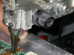
HotBar02s <-- Thermode


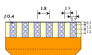
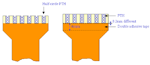
The common conductor inside FPC is building Plating hole (PTH) on contact finger of FPC as below sketch. Three PTHs on each contact finger are preferable. One half-circle via + two circle vias can be acceptable if there is no space for three completed vias.
HotBar_PTH_thumb1

It is necessary to apply double adhesive to fix FPC on board during Hot-Bar reflow process. No body like to take the hot touch risk to hold FPC on PCB for Hot Bar process.

To summary the requirements for Hot-Bar FPC:

  • 3 PTHs on Hot-Bar finger.
  • Double adhesive at near side to stick flex cable on PCB before Hot Bar process. The thickness should be less than 0.15mm and leave 0.2mm space from Hot-Bar terminal. 

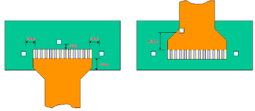
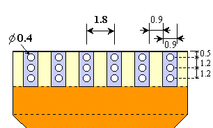
Hot-Bar PCB pattern size should be designed as below to prevent solder short between patterns while thermode press down.
HotBar_cable_pitch_thumb


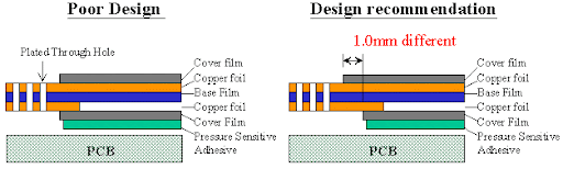
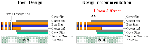
In order to prevent FPC from broken at solder finger edge. It is recommended to make different cover films (polymide) with various length end to fix the stress concentration issue. Detail recommended structure show as below.
hotbar_flex_cable1_thumb5


The recommended components distance from Hot-Bar land pattern:

  • The minimum distance from components to front side of FPC is 2mm.
  • The minimum distance from components to both sides of PCB is 3mm.
  • The minimum distance from PCB edge to contact pads of FPC is 5mm. (This 5mm is for double adhesive tape purpose)
  • The minimum distance from components to contact pads under FPC is 10mm. (This 10mm is for double adhesive tape fixing on PCB)
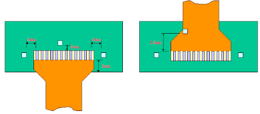
HotBar_PCB_thumb1


我的網誌清單