The PTF (Polymer Thick Film) uses silkscreen to print the silver and carbon combination conductive inks on PET (Polyethylene terephthalate) substitute to reach low cost purpose as compare with FPC (Flexibility printing Circuit). Unfortunately, the screen-printing has some ability limits.
Below are my experiences to show you some notices for the screen-printing process.
- Foreign particle contamination: The particle may come from the air or inks, include conductive and dielectric inks. In order to control the particle around the air, A 100K class of clean room is preferable for screen-printing process fields. Using filter to screen out big particle inside inks is also recommended.
You can image the insulation particle locates on the circuit trace will bring the trace open or increase the resistance. The conductive particle locates between the circuit traces will make trace short. Especially, while you are manufacturing the fine pitch, pitch less than 16 mils (0.4mm), products.
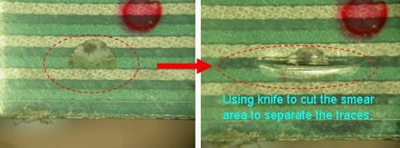
If the particle come from inks then it may clog the mesh of silkscreen template then bring the printing skip and result circuit open. Sometimes particle will pierce the dielectric layer between conductive layers and bring the circuit short between conductive layers. - Printing smear on circuits layer: Printing smear defect is a commonly problem for screen-printing process. It will make short between circuits once the smear cross to adjacent circuit traces. Especially for fine pitch products. Sometimes you hard to detect this kind of defect by test fixture and it will show up circuit short defect after it install unit for a period. it is highly suspected the electromigration happens between circuit traces.
It better to clean the silkscreen template regularly base on actual status and check the printing result every layer after every circuits printing. It will be good if factory can implement the AOI (Auto Optical Inspector) equipment to inspect printing quality.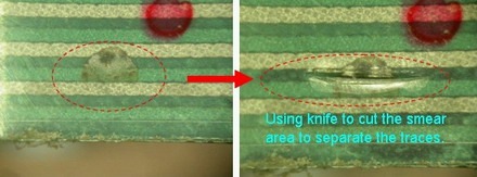
(↑The printing smear between circuits and bring electric short after environmental test. Using knife to cut off the smear area then PTF back to work.) - Printing voids on dielectric layer: There are some tiny voids under screen-printing ink. Once the voids locate on the circuits between two conductive then it may bring circuit short. My experience show the eletromigration will grow dendrite between the layers of circuits through voids if you give voltage as engine and moisture as accelerator.
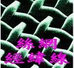
You may reduce the viscosity for dielectric ink to solve the dielectric voids. Printing two or three dielectric layers between electric circuits and using different screen template with different mesh count and angle to cover the voids are preferred.

More article:
PTF(Polymer Tick Film) introduction
Hot-Bar FPC Design Notices